
Programmable Inductive Proximity Detector SoC ASIC
The semiconductor industry has come a long way since the advent of simple custom chips. Today, entire systems can be integrated on one chip, hence the term System-on-a-Chip or SoC has been coined. This term can mean different things for different products but typically it will mean that the majority of the electronics are integrated into one ASIC, or several ASICs in the case of large systems.
At LMI, our SoCs typically contain of all or most of the analog and/or RF electronics, power management functions, data acquisition circuits (sample-hold, track-hold, ADC, and/or DAC), system memory (non-volatile for program memory, trimming, user options), ROM (optional), RAM, and digital processing – either a microprocessor or DSP.
Two years ago, a subsidiary of a large international firm contracted with LMI to develop and manufacture an SoC for a new product in the industrial automation space. This chip had to be small and low cost to achieve the expected sales of millions of units per year. The primary function is an inductive proximity detector that uses two oscillators – a reference oscillator and a detector oscillator. The concept of operation is as follows: the two oscillators are locked together in frequency and phase at calibration. When a conductive material, either ferrous or non-ferrous, approaches the detector oscillator, the phase and/or amplitude of the detector oscillator changes and can be precisely detected to determine the proximity of the subject material.
The SoC signal path contains the oscillator circuitry, detectors for phase and peak detection, demodulation and amplification, a 10-bit ADC, a temperature sensor, reference voltage generator, and calibration circuitry. On-chip power management includes a voltage regulator and a power-on reset. The circuit has a number of modes of operation (including 2 or 3 wire), and various user features. To handle these different modes, the circuit has an on-chip 8051 microprocessor, 7 kilobytes of non-volatile program memory, and 256 bytes of static single port RAM. Users in the field can program the chip via a serial port using Manchester coded data. The quiescent current is limited to a maximum of 2 mA in all modes of operation.
The customer had a well-defined set of requirements and had built discrete circuitry to prove the basic concepts of the product prior to the start of the project. However, as the first step of the
project, a top-level circuit architecture had to be developed along with detailed design specifications to guide the SoC development. This specification included all firmware requirements, which was the responsibility of LMI to develop. This firmware is programmed into each ASIC during production testing.
Once the architecture and specifications were defined, including specs for each of the sub-blocks, the project was divided into analog, digital and firmware sections that were assigned to various members of the design engineering team. Extensive analog, digital and mixed-signal simulations were run during the design process to ensure that the overall system would perform as needed. Test engineering participated heavily in the design of the chip testability – this is a very important part of any SoC development.
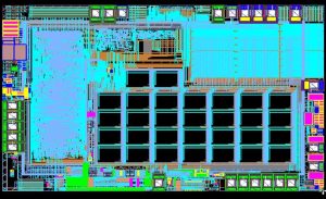
The first prototypes were fully functional due to the extensive design methodology employed. There were some minor problems which were able to be changed with only upper layer metal layers. The process used is a X-FAB 180 nm BiCMOS, the die size is 4.8 mm2 and the package is a 4 mm x 4 mm, 24 lead QFN.
