
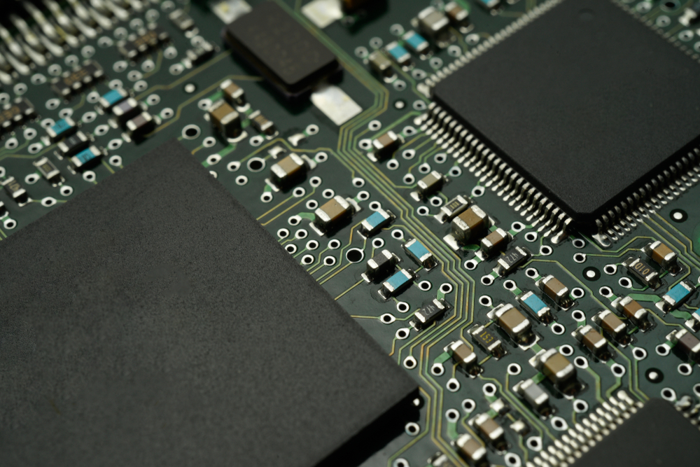
Designing for Low Power in the ASIC Chip
In the rapidly advancing world of electronics, the demand for energy-efficient devices is greater than ever. ASICs are at the forefront of this innovation, powering everything from smartphones to medical devices. Designing an ASIC chip for low power consumption is crucial to meet the needs of modern applications, ensuring longer battery life, reduced heat generation, and enhanced performance. Here, we explore various techniques to optimize power consumption in ASIC design.
Clock Gating: Reducing Dynamic Power Consumption
One of the most effective techniques for reducing power consumption in ASIC chips is clock gating. This method targets dynamic power consumption, which is the power the circuit consumes when it is actively switching states.
How Clock Gating Works: Clock gating reduces power consumption by disabling the clock signal to portions of the circuitry that are not in use. By preventing unnecessary toggling of transistors, clock gating minimizes the dynamic power wasted in idle sections of the chip. Implementing clock gating requires identifying circuit parts that can turn off without affecting the overall functionality, such as certain logic blocks or processing units.
Benefits of Clock Gating: The primary benefit of clock gating is the significant reduction in dynamic power consumption, which can account for a substantial portion of the total power usage in an ASIC chip. Additionally, clock gating can improve the chip’s overall efficiency, leading to better performance and lower heat generation.
Challenges and Solutions: While clock gating is effective, it introduces complexity into the design process. Designers must carefully manage the timing and control signals to ensure that the clock is gated accurately without introducing glitches or timing errors. Advanced design tools and techniques, such as automated clock gating synthesis, can help streamline this process and ensure reliable implementation.
Power Gating: Minimizing Static Power Consumption
Power gating is another crucial technique for optimizing power consumption in an ASIC chip. This method addresses static power consumption, which is the power the circuit consumes when it is not actively switching states but still consuming power due to leakage currents.
How Power Gating Works: Power gating reduces static power consumption by completely shutting off power to inactive chip sections. This is achieved by inserting sleep transistors between the power supply and the circuit blocks that can be powered down. When these transistors turn off, the power supply is cut off, eliminating leakage currents and reducing static power consumption.
Benefits of Power Gating: Power gating offers significant reductions in static power consumption, especially in modern semiconductor technologies with substantial leakage currents. By effectively managing idle periods, power gating extends battery life and reduces power usage in portable and wearable devices.
Challenges and Solutions: Power gating requires careful design to ensure a smooth transition between active and sleep modes and not affect the chip’s performance. This involves managing wake-up times, ensuring data retention in power-gated blocks, and designing robust control mechanisms. Advanced power management strategies and simulation tools can assist designers in overcoming these challenges.
Voltage Scaling: Optimizing Power and Performance
Voltage scaling is another powerful technique for optimizing power consumption in ASIC chips. This method involves adjusting the supply voltage to balance power consumption and performance requirements.
How Voltage Scaling Works: Voltage scaling reduces power consumption by lowering the supply voltage to the minimum level required for the desired performance. Dynamic Voltage and Frequency Scaling (DVFS) is a common approach. In this approach, the voltage and frequency are adjusted based on the workload. When the demand is low, the voltage and frequency can be reduced, leading to lower power consumption.
Benefits of Voltage Scaling: Voltage scaling offers a flexible and efficient way to manage power consumption dynamically. It allows for significant power savings during periods of low activity while maintaining high performance when needed. This makes it ideal for applications with variable workloads, such as mobile devices and adaptive computing systems.
Challenges and Solutions: The primary challenge with voltage scaling is ensuring the circuit operates reliably at lower voltages. This requires careful power distribution network design, robust timing analysis, and thorough testing to avoid timing violations and signal integrity problems. Leveraging advanced voltage scaling techniques and design tools can help address these challenges effectively.
Conclusion
Designing ASIC chips for low power consumption is essential in today’s energy-conscious world. Techniques like clock gating, power gating, and voltage scaling are vital in optimizing power efficiency while maintaining performance. By implementing these strategies, designers can create highly efficient ASIC chips that meet the demands of modern applications, extending battery life, reducing heat, and enhancing overall device performance. As a leading microsystems company, staying at the forefront of these low-power design techniques is crucial for driving innovation and delivering cutting-edge solutions.
Learn all about Linear MicroSystems by clicking here!
Linear MicroSystems, Inc. is proud to offer its services worldwide as well as the surrounding areas and cities around our Headquarters in Irvine, CA: Mission Viejo, Laguna Niguel, Huntington Beach, Santa Ana, Fountain Valley, Anaheim, Orange County, Fullerton, and Los Angeles.


