RF ASICs for Wireless Sensor Networks: Enabling Smart Environments
As the world becomes increasingly connected, WSNs are playing a central role in enabling smart environments across industries. From smart cities and industrial automation to environmental monitoring and healthcare, these networks rely on seamless, low-power communication between distributed devices. At the heart of this capability is the RF ASIC, a specialized integrated circuit designed to handle radio frequency communication with high efficiency and precision.
The Role of RF ASIC in Wireless Sensor Networks
Wireless sensor networks consist of numerous sensor nodes that collect and transmit data over the air. Each node must be capable of reliable communication while operating under strict power and size constraints. This is where the RF ASIC becomes essential.
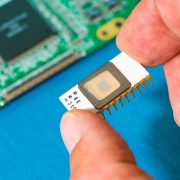
An RF ASIC integrates critical radio-frequency components, such as transmitters, receivers, frequency synthesizers, and power amplifiers, into a single chip. Consolidating these functions reduces the need for external components, minimizing signal loss and improving overall system reliability. This integration also enables tighter control over performance parameters like frequency stability, sensitivity, and noise reduction.
In WSN applications, they’re often designed to support specific communication protocols such as Bluetooth Low Energy, Zigbee, LoRa, or proprietary low-power standards. These tailored designs ensure optimal performance for the intended use case, whether it’s short-range indoor connectivity or long-range outdoor communication.
Equally important is power efficiency. Many wireless sensor nodes are battery-powered or energy-harvesting, requiring components that can operate for extended periods without maintenance. RF ASICs are engineered to deliver ultra-low power consumption, enabling long device lifespans while maintaining consistent connectivity.
Enabling Smart and Scalable Environments
The integration capabilities of the RF ASIC are a key enabler of scalable and intelligent wireless sensor networks. In smart cities, for example, RF ASIC-powered sensors monitor traffic flow, air quality, and infrastructure health in real time. These systems rely on efficient data transmission to central platforms where insights can be generated and acted upon.
In industrial settings, RF ASICs support the deployment of wireless monitoring systems that track equipment performance, detect anomalies, and enable predictive maintenance. By eliminating the need for extensive wiring, these solutions reduce installation costs and increase flexibility in dynamic environments.
Smart agriculture is another area where they’re making a significant impact. Wireless sensor networks equipped with RF ASIC technology can monitor soil moisture, temperature, and crop conditions, helping farmers optimize irrigation and improve yields. Similarly, in healthcare, RF ASIC-enabled devices facilitate remote patient monitoring, allowing for continuous data collection and timely interventions.
The scalability of these networks depends heavily on the reliability and efficiency of the RF ASIC. As the number of connected devices grows, maintaining robust communication becomes increasingly complex. Advanced designs address this challenge by incorporating features such as adaptive frequency control, interference mitigation, and secure data transmission.
The Future of RF ASIC in Smart Connectivity
Looking ahead, the evolution of the RF ASIC will continue to drive innovation in wireless sensor networks. Advances in semiconductor processes and design techniques are enabling even greater levels of integration, allowing RF ASICs to combine analog, digital, and mixed-signal components on a single chip.
Emerging technologies such as edge computing and artificial intelligence are also influencing RF ASIC development. Future designs will not only handle communication but also support local data processing and decision-making, reducing latency and bandwidth requirements.
As industries continue to embrace digital transformation, the demand for efficient, reliable, and scalable wireless connectivity will only grow. The RF ASIC is a foundational technology in this landscape, enabling the development of smarter, more responsive, efficient, and interconnected environments.
Conclusion
The RF ASIC is a critical enabler of wireless sensor networks, providing the performance, efficiency, and integration needed to support smart environments. By facilitating reliable communication and low-power operation, RF ASICs are helping to unlock new possibilities across a wide range of applications. For microsystems companies, investing in advanced RF ASIC design is key to driving innovation and meeting the demands of an increasingly connected world.
Learn about our work at Linear MicroSystems by clicking here!
Linear MicroSystems, Inc. is proud to offer its services worldwide as well as the surrounding areas and cities around our Headquarters in Irvine, CA: Mission Viejo, Laguna Niguel, Huntington Beach, Santa Ana, Fountain Valley, Anaheim, Orange County, Fullerton, and Los Angeles.