
Integrating RF Components into a System on a Chip: What Engineers Need to Know
As wireless connectivity becomes a standard requirement across industries, from IoT and healthcare to automotive and aerospace, the need to integrate RF (radio frequency) functionality directly into an ASIC Chip has grown significantly. Combining RF components within a System on a Chip (SoC) reduces size, lowers power consumption, and enhances overall system performance. However, RF integration introduces a unique set of challenges that engineers must carefully address to ensure success.
Understanding the technical considerations and best practices is key to developing a reliable, high-performing ASIC Chip with integrated RF capabilities.
Design Considerations for RF Integration
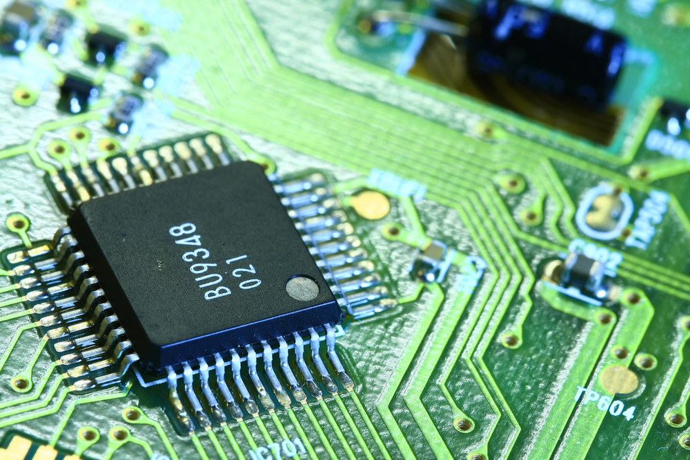
Integrating RF components into an ASIC Chip requires a deep understanding of both analog and digital design principles. RF circuits such as amplifiers, mixers, oscillators, and filters are highly sensitive to noise, interference, and layout conditions. Unlike purely digital components, RF elements must operate within precise frequency ranges and are more susceptible to environmental variations.
One of the primary challenges is managing signal integrity. Parasitic effects, electromagnetic interference (EMI), and substrate noise can significantly degrade RF performance. Engineers must carefully isolate RF blocks from noisy digital sections of the ASIC Chip through layout techniques such as guard rings, shielding, and dedicated power domains.
Process technology selection is another critical factor. Not all semiconductor processes are optimized for RF performance, so choosing a process that supports both RF and digital integration is essential. Technologies like RF CMOS and SiGe BiCMOS are commonly used to balance cost, performance, and integration requirements.
Additionally, impedance matching and proper routing are crucial for minimizing signal loss and maximizing efficiency. Even small layout variations can impact performance, making precision in design and simulation a top priority.
Simulation, Verification, and Testing | ASIC Chip
Given the complexity of RF behavior, simulation and verification play a vital role in ensuring that an ASIC Chip performs as intended. Engineers must use advanced modeling tools to simulate RF circuits under various operating conditions, including temperature changes, voltage fluctuations, and signal interference.
Co-simulation of RF and digital components is particularly important, as interactions between these domains can introduce unexpected issues. Verifying the entire system holistically helps identify potential bottlenecks and ensures seamless integration.
Once the design is finalized, testing becomes the next critical step. RF testing differs from traditional digital validation, requiring specialized equipment and methodologies to measure parameters such as gain, noise figure, linearity, and frequency response. Engineers must design test structures and access points into the ASIC Chip early in the development process to facilitate accurate measurements.
Calibration and tuning may also be necessary post-fabrication to optimize performance. This is especially important in applications where precision and reliability are critical, such as medical devices or communication systems.
Best Practices for Successful RF SoC Development
To successfully integrate RF components into an ASIC Chip, engineers should adopt a holistic and collaborative approach. Early alignment between RF, analog, and digital teams helps prevent integration challenges later in the process. Clear specifications, robust simulation strategies, and careful layout planning are all essential for achieving optimal performance.
It’s also important to consider power management, as RF components can significantly impact overall energy consumption. Efficient design techniques and low-power architectures can help balance performance with battery life, particularly in portable and IoT devices.
Finally, partnering with experienced microsystems providers can accelerate development and reduce risk. Their expertise in RF design, fabrication processes, and testing methodologies can help ensure a smoother path from concept to production.
As wireless technologies continue to evolve, the ability to integrate RF functionality into an ASIC Chip will remain a key differentiator for innovative products. By understanding the challenges and applying best practices, engineers can create highly integrated solutions that meet the demands of today’s connected world.
Linear MicroSystems, Inc. is proud to offer its services worldwide as well as the surrounding areas and cities around our Headquarters in Irvine, CA: Mission Viejo, Laguna Niguel, Huntington Beach, Santa Ana, Fountain Valley, Anaheim, Orange County, Fullerton, and Los Angeles.


