
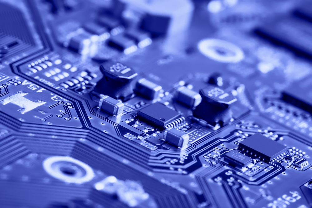
Microsystem Integration and Packaging Techniques
Microsystems play a pivotal role in advanced electronics by combining microelectromechanical systems (MEMS), microelectronics, and other miniaturized components into highly functional devices. Their success relies heavily on sophisticated integration and packaging techniques that ensure performance, reliability, and efficiency. Here, we delve into the latest trends and innovations in microsystem integration and packaging.
Advanced Integration Techniques for Microsystems
Effective microsystem integration combines various components, such as sensors, actuators, and electronics, into a cohesive unit. This process demands precision and innovation to achieve the desired functionality and miniaturization.
System-on-Chip (SoC) Integration: One of the most significant advancements in microsystem integration is developing System-on-Chip (SoC) technology. SoC integrates electronic circuits and components onto a single silicon chip. This approach reduces the size and power consumption of microsystems while enhancing performance. SoCs are particularly beneficial in applications such as wearable devices, medical implants, and IoT sensors, where space and energy efficiency are critical.
Heterogeneous Integration: Another key trend in microsystem integration is heterogeneous integration, which combines different components and materials onto a single substrate. This technique enables the integration of MEMS devices with traditional silicon-based electronics, optical components, and even biological elements. Heterogeneous integration allows for the creation of multifunctional microsystems that perform complex tasks, such as environmental monitoring, health diagnostics, and advanced computing.
3D Integration: 3D integration revolutionizes microsystem design by stacking multiple layers of components vertically. This technique increases the density of the microsystem, allowing more functionality within a smaller footprint. By shortening the interconnects between layers, 3D integration enhances signal speed and reduces power consumption. This approach is essential for high-performance applications like advanced sensors, imaging systems, and communication devices.
Innovative Packaging Techniques for Microsystems
Packaging is critical to microsystem development, as it protects delicate components from environmental factors and ensures reliable operation. Modern packaging techniques are evolving to meet the demands of increasingly complex and miniaturized microsystems.
Wafer-Level Packaging (WLP): Wafer-level packaging involves packaging the microsystem components at the wafer level before they are diced into individual units. This method offers several advantages, including reduced package size, improved thermal management, and lower production costs. WLP is widely used in MEMS devices, RF components, and optical sensors, where precision and efficiency are paramount.
System-in-Package (SiP): System-in-Package (SiP) technology encapsulates multiple integrated circuits and passive components into a single package. Unlike SoC, SiP allows for the integration of chips from different technologies and vendors. This flexibility makes SiP ideal for complex applications that require diverse functionalities, such as smartphones, medical devices, and automotive electronics. SiP also simplifies the design process and accelerates time-to-market for new products.
Flip-Chip Technology: Flip-chip technology is gaining traction in microsystem packaging due to its ability to provide high-density interconnections and excellent electrical performance. In flip-chip packaging, the microsystem components are mounted upside-down on the substrate, allowing direct electrical connections through solder bumps. This technique minimizes the interconnect length, reducing signal loss and improving thermal management. Flip-chip packaging is commonly used in high-speed computing, telecommunication devices, and advanced sensors.
Conclusion
Microsystem integration and packaging are critical processes that determine modern electronic devices’ functionality, performance, and reliability. Advanced techniques such as SoC, heterogeneous integration, and 3D integration push the boundaries of what microsystems can achieve. At the same time, innovative packaging methods like wafer-level packaging, system-in-package, and flip-chip technology ensure these complex systems are protected and efficient.
As a leading microsystem company, staying abreast of these emerging trends and adopting the latest integration and packaging technologies is essential. By leveraging these advancements, we can develop next-generation microsystems that meet the growing demands of various industries, from healthcare and consumer electronics to automotive and aerospace, driving innovation and enhancing the quality of life.
Learn more about MicroSystems by clicking here!
Linear MicroSystems, Inc. is proud to offer its services worldwide as well as the surrounding areas and cities around our Headquarters in Irvine, CA: Mission Viejo, Laguna Niguel, Huntington Beach, Santa Ana, Fountain Valley, Anaheim, Orange County, Fullerton, and Los Angeles.


