
Quality Performance Aspects to Look For In RF ASICs
There are a set of challenges in the development of RF ASICs, which could be beyond those encountered in baseband IC design. One of the most basic challenges is the demand it puts on the process technology.
High-Performance Passives
Aside from the fast transistors needed, high-performance passives are among those that have minimal factors that would minimize crosstalk and bandwidth reduction. For this reason, high Q inductors are needed in the process.
Performance specifications of the RF ASIC will typically drive the implementation into deep submicron processes which are optimized for RF performance. At the same time, development time will be longer due to the fact that there are extensive simulations necessary for the consideration of the impact of parasitics.
Moreover, some design iteration be it electrical or physical is necessary to account for these layout parasitics. In this case, RF ASICs would require larger non-recurring engineering budget for the process constraints and amount of the engineering resources needed.
Testing RF ASICs
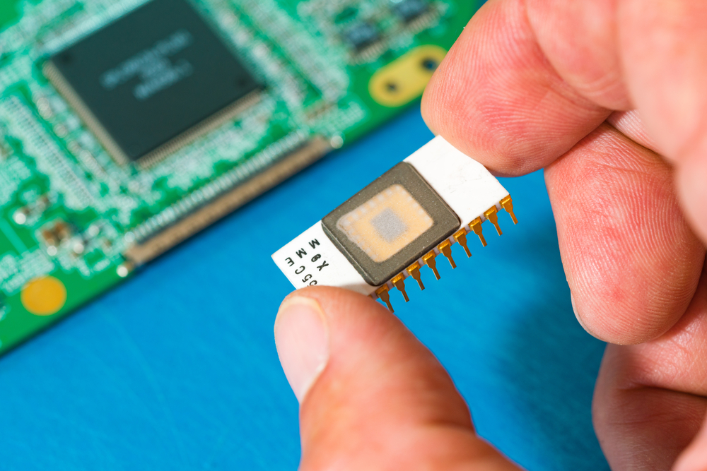
The wafer-level testing process for RF ASICs should also be a factor in performance. Basically, they are sold in die form as they are part of the chip-on-board packaging technology. Therefore, wafer testing is necessary for RF frequencies.
Thus, special probe cards and prober hardware are necessary, including the knowledge of the test team having RF background. So a carefully designed tester interface hardware must be used. They must be fabricated to have a minimal impact of stray parasitics and mismatch on measurements.
Design Architecture Parameters
The design team must also choose the appropriate architecture and come up with a reasonable set of requirements to match the target budget and schedule aside from the product requirements. Therefore, it is required to conduct an investigation phase in RF ASICs around 2-6 weeks based on the customer to come up with a more satisfactory project plan.
Design Parameters to Be Considered In Investigation Phase
- Available power or DC power supply
- Full or half-duplex operation
- Receiving and transmitting frequencies and IBW or instantaneous bandwidth
- Receiver input and transmitter output dynamic range
- On and off-chip filtering
- Frequency planning for receiver and transmitter
- Number of channels
- Channel to channel isolation
- DC power dissipation
- Transmitter power, receiver sensitivity, peak to average ratio, and efficiency
- Attenuation or automatic gain control
- ESD impact
The architectural approach of RF ASIC and the integrated circuit process choice are greatly influenced by these parameters. These are required to create a link budget for the development of specifications in individual ASIC circuit blocks.
The RF circuitry is often part of the larger system-on-a-chip wherein there is importance in noise immunity and crosstalk. Therefore, it should be well considered to have an overall physical layout of the chip. At the same time, great care must be given to the power supply routing scheme, including the location and number of power and grounds.
Thus, it is always important to pay attention to the design considerations and the process and testing requirements offered by ASIC companies having extensive expertise in RF.
Linear MicroSystems, Inc. is proud to offer its services worldwide as well as the surrounding areas and cities around our Headquarters in Irvine, CA: Mission Viejo, Laguna Niguel, Huntington Beach, Santa Ana, Fountain Valley, Anaheim, Orange County, Fullerton, and Los Angeles.


