The Evolution of Analog Design: From Simple Circuits to Complex Systems
Analog Design has been a foundational element of electronics since the earliest days of electrical engineering. Long before digital systems dominated the technology landscape, analog circuits were responsible for amplifying signals, regulating power, and enabling communication across vast distances. Over time, Analog Design has evolved dramatically, shifting from simple, discrete components to highly integrated solutions that power today’s complex semiconductor systems. Understanding this evolution offers valuable insight into why analog expertise remains essential in modern microsystems.
Early Foundations of Analog Design
The origins of Analog Design date back to the late 19th and early 20th centuries, when engineers relied on basic components such as resistors, capacitors, inductors, and vacuum tubes. Early analog circuits were used in radios, telephones, and early power systems, where continuous electrical signals represented sound, light, or motion. These designs were largely handcrafted, requiring deep intuition and hands-on experimentation.
The invention of the transistor in the late 1940s marked a turning point for Analog Design. Transistors replaced bulky vacuum tubes, enabling smaller, more reliable, and more energy-efficient circuits. During this era, analog engineers focused on amplifiers, oscillators, and filters that formed the backbone of early consumer electronics and industrial control systems. Despite their relative simplicity, these circuits required precision, as small variations in component values could significantly affect performance.
The Rise of Integrated Circuits and Mixed-Signal Systems
As semiconductor manufacturing advanced in the 1960s and 1970s, Analog Design entered a new phase with the introduction of integrated circuits (ICs). Instead of assembling discrete components, engineers could now integrate multiple analog functions onto a single chip. This innovation improved consistency, reduced cost, and enabled entirely new applications.
With the growth of digital computing, Analog Design did not disappear; instead, it became more critical. Modern systems rely on mixed-signal designs that combine analog and digital circuitry on the same silicon. Analog circuits handle real-world signals such as voltage, current, temperature, and radio-frequency signals, while digital logic processes and interprets data. Designing these systems requires balancing noise, power efficiency, and signal integrity, making Analog Design more complex and specialized than ever before.
Modern Applications in Complex Semiconductor Systems
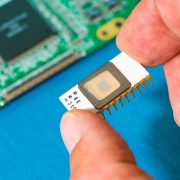
Today, Analog Design plays a vital role in advanced microsystems across industries such as automotive, medical devices, telecommunications, and renewable energy. High-performance analog blocks are essential for sensors, data converters, power management ICs, and RF communication systems. As semiconductor nodes shrink and systems become more integrated, analog engineers face challenges such as reduced voltage headroom, increased interference, and stricter performance requirements.
Despite these challenges, Analog Design continues to evolve through innovative architectures, advanced simulation tools, and close collaboration between design and process engineering teams. In an increasingly digital world, analog circuits remain the critical bridge between physical phenomena and digital intelligence.
Looking Ahead
The evolution of Analog Design reflects the broader history of electronics, one of constant adaptation and innovation. From simple circuits built with discrete components to sophisticated systems-on-chip, analog engineering remains indispensable. As microsystems grow more complex, the demand for skilled Analog Design will continue to rise, ensuring its continued relevance.
Learn about our work at Linear MicroSystems by clicking here!
Linear MicroSystems, Inc. is proud to offer its services worldwide as well as the surrounding areas and cities around our Headquarters in Irvine, CA: Mission Viejo, Laguna Niguel, Huntington Beach, Santa Ana, Fountain Valley, Anaheim, Orange County, Fullerton, and Los Angeles.