Advancements in RF ASIC Design: Enhancing Wireless Communication Systems
Wireless communication systems are at the heart of today’s connected world. From smartphones and smart homes to automotive and healthcare applications, reliable wireless connectivity drives innovation across industries. Behind the scenes, RF ASIC technology plays a pivotal role in enabling these advancements. By combining specialized design with high-performance functionality, RF ASICs are transforming the way devices communicate, improving efficiency, speed, and reliability.
The Importance of RF ASIC in Modern Connectivity
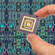
At its core, an RF ASIC integrates multiple radio-frequency components into a single, custom-designed integrated circuit (IC). This enables the development of smaller, more efficient devices compared to using separate, off-the-shelf components. By tailoring circuits to specific applications, RF ASICs can deliver optimized performance while consuming less power—an essential advantage for today’s battery-powered devices.
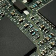
In wireless communication systems, RF ASICs handle critical tasks such as signal transmission, reception, filtering, and amplification. These functions ensure that signals are clear, strong, and free of interference. As wireless networks become increasingly complex, from 5G deployment to satellite communications, the precision and efficiency of RF ASIC design directly impact the quality of connectivity.
For consumer electronics, this translates to faster data transfer, smoother streaming, and longer battery life. In industrial and automotive contexts, RF ASICs enable low-latency communication and highly reliable links, which are crucial for safety and automation.
Advancements Driving RF ASIC Innovation
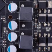
Recent progress in RF ASIC design is addressing both performance demands and industry challenges. One key area of innovation is integration. Designers are combining analog, digital, and RF circuitry into mixed-signal ASICs that reduce system complexity and cost. This high level of integration also minimizes signal loss and interference, improving overall reliability.
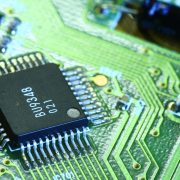
Another advancement lies in the use of advanced semiconductor processes. By leveraging smaller geometries, RF ASICs can operate at higher frequencies, supporting next-generation wireless standards like 5G and beyond. These chips are also more energy-efficient, making them ideal for mobile devices, IoT sensors, and wearables where power consumption is a constant concern.
Additionally, adaptive design techniques are emerging. RF ASICs can now be engineered to adjust dynamically to changing environments, such as varying frequencies or interference levels. This adaptability ensures stable communication across diverse conditions, which is particularly valuable for applications in the automotive, aerospace, and defense sectors.
The Future of Wireless Systems with RF ASICs
As wireless technologies continue to evolve, RF ASIC development will remain a central component of innovation. The rollout of 6G, the expansion of IoT ecosystems, and the growing need for low-latency, high-reliability communication will drive demand for advanced RF ASICs. These chips will need to support higher bandwidths, improved energy efficiency, and enhanced security.
For businesses and consumers alike, the result will be seamless, always-on connectivity that supports everything from autonomous vehicles to telemedicine. By bridging performance and customization, RF ASIC design ensures wireless communication systems are prepared for the demands of tomorrow.
RF ASIC Wrap Up
The evolution of wireless communication depends heavily on advancements in RF ASIC technology. By enabling efficient, reliable, and adaptable systems, RF ASICs are the foundation for the next generation of connectivity. As innovation accelerates, these specialized chips will continue to enhance the performance of devices and networks across industries, ensuring a more connected and intelligent world.
Keep learning from Linear MicroSystems experts by clicking here!
Linear MicroSystems, Inc. is proud to offer its services worldwide as well as the surrounding areas and cities around our Headquarters in Irvine, CA: Mission Viejo, Laguna Niguel, Huntington Beach, Santa Ana, Fountain Valley, Anaheim, Orange County, Fullerton, and Los Angeles.