
General Design Steps for Analog IC Design
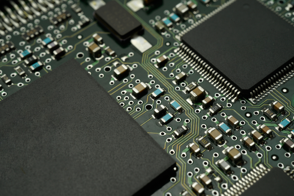
Integrated Circuit is the little black chip embedded in an electronic device. This flat black chip or commonly known as a silicon chip, or analog IC, is made of electronic components such as transistors, resistors, capacitors, and others to work together to perform a specific function.
Integrated Circuits (ICs) are vital components in telecommunications, automotive, aerospace, Internet, multi-media, and other applications in today’s modern world. Integrated Circuit designs are divided into 2 categories: analog and digital.
Digital Integrated Circuit (IC) is specifically designed to produce components like RAM and microprocessors; it is mainly for logical functions. On the other hand, Analog IC focuses on the physics of semiconductor devices.
The analog design is mainly to continuously manipulate varying electrical signals through the use of amplifiers and filters.
Analog IC Design
Analog ASIC design starts with product specification, circuit design and architecture, logic design, physical design, physical verification
- Specification – Analog IC specification phase involves market surveys; determining potential customers, and predict future needs. Gauging future demands will also influence how you would like to do with your ASIC, and working on the requirements for the product to appeal better to customers.
- Design and Architecture – this stage involves discussion on the pros and cons of the design including performance and functional implications, time, and cost allocation. The design and architecture phase involves technical and functional details.
- Logic design – the logical and verification phase involves the coding of the data flow of the individual functional block using Verilog, system Verilog, or VHDL. The logic design includes combination logic, sequential Elements, finite State Machines (FSMs), arithmetic Logic Blocks, data-path Design, and Analog Design.
- Physical design – this stage focuses on the backend design cycle. The phase is sub-divided into synthesis, floor planning, placement, clock tree synthesis, detail routing, physical verification.
- Synthesis translates the RTL code into standard cell gates.
- Floorplanning is when engineers follow the analog ASIC design by dividing the area into partitions. Functional blocks, pins, and ports are also integrated into the floor planning phase. The process also determines the size of the chip, wire length, and functionality. Good floor planning is essential to eliminate or at least minimize issues in the signal, routing, and total chip area.
- Placement involves the optimal placement of all standard cells in the chip.
- The clock three synthesis processes are meeting the time, power, and area requirements. This step is used to ensure that optimal clock latency is achieved while lowering power consumption.
- Detail routing is the stage involves multiple types of researches to ensure detours are minimized that can cause implications on timing. This process also ensures that Design Rule Check violations are at a minimum.
- Physical verification is all about making sure that the layout is parallel to the way it is designed to. This is also to avoid any errors before the tape out.
Analog ASIC design is complicated; and will continue to progress along with technology. Analog IC design is an integral part of today’s modern life. Life has never been the same since the invention of Integrated Circuits.
Linear MicroSystems, Inc. is proud to offer its services worldwide as well as the surrounding areas and cities around our Headquarters in Irvine, CA: Mission Viejo, Laguna Niguel, Huntington Beach, Santa Ana, Fountain Valley, Anaheim, Orange County, Fullerton, and Los Angeles.


