
What is VLSI and its relation to ASIC chips
What are VLSI and its uses?
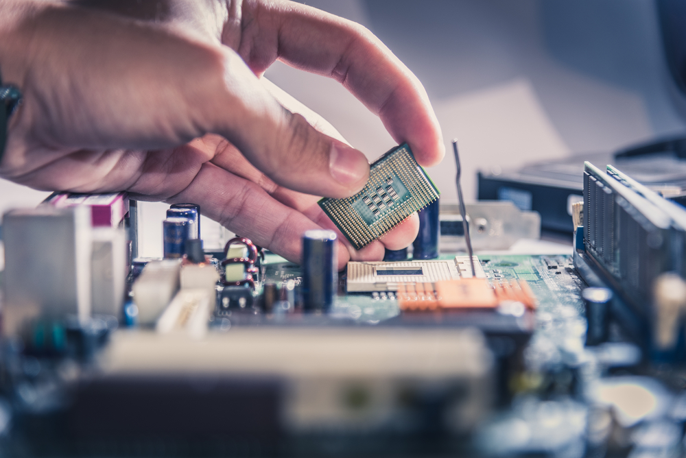
Very Large Scale Integration (VLSI) is the process of creating an Integrated Circuit (IC) by incorporating tens of thousands of transistors into one single chip. VLSI reduces the need for more circuits in one system, especially for complex devices. The integration of technology helped reduce the size of electronic devices without affecting efficiency.
VLSI technology was developed in the 1970s when cutting edge computer processor microchips were under improvement. Today, it is a widely utilized technology for microchip processors and incorporated circuits (IC). Very
Large Scale Integration was initially designed to support a huge number of transistor entryways on a microchip. These transistors are integrated and implanted inside a microchip, which significantly reduced its size yet still can hold big numbers of transistors.
Back in the days of the vacuum tube method, electronic devices were bulky and require more power. And due to the wastage of heat and power, efficiency is decreased. The advancement of technology and electronic devices brought forth the invention of VLSI. The method helped accommodate the growing requirements of complex designs; to fabricate all components onto a single chip.
VLSI design flow
There are 3 major stages in the VLSI design process; behavioral, logic circuit, and layout representations.
- Behavioral representation is the first step. The process involves identifying the functionality of the device and how it is going to communicate with the exterior. A Hardware Description Language (HDL) is used to establish the behavior of the device.
- Logic circuit representation works by using functional blocks from cell libraries to integrate the behavioral representation of the VLSI design into a logic circuit representation. Once verified, the gate-level netlist is generated to develop the design layout.
- Layout representation is the final stage which determines the placing and routing of the chips. Once arranged at their best locations, building blocks are then interconnected.
Uses in today’s advance word:
- Computers
- Commercial electronics
- Medicine
- Automobiles
- Digital signal processing
What is ASIC?
Application Specific Integrated Circuit (ASIC) is designed for one specific application only. It is a microchip designed to one special application like a pocket-sized computer. It is widely used in the design and manufacturing of electronic devices. Some examples of popular ASIC chip include a chip with microprocessor for cellular phones to work, a chip for a satellite, a chip for a talking toy bear, and a chip used for the voice recorder.
ASICs can be custom manufactured for specific client applications or pre-manufactured for a special product or application.
Types of ASIC chip designs
- Full custom design
- Semi-custom design
- Programmable ASIC
Very Large Scale Integration (VLSI) and Application Specific Integrated Circuit (ASIC)
So, VLSI involves the development of ASIC. For specific applications, special chips are designed which is also called Application Specific Integrated Circuit (ASIC). These specialized chips changed the way electronic devices are designed and manufactured.
This method is expensive, but several industries are using this technology because this can be reconfigured if needed. Using ASIC, you can map any design, develop a design that can be modified multiple times.
Linear MicroSystems, Inc. is proud to offer its services worldwide as well as the surrounding areas and cities around our Headquarters in Irvine, CA: Mission Viejo, Laguna Niguel, Huntington Beach, Santa Ana, Fountain Valley, Anaheim, Orange County, Fullerton, and Los Angeles.


