System On a Chip

Powering the Next-Gen IoT: The Indispensable Role of Low-Power ASICs and SoCs

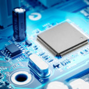
The rapid growth of the Internet of Things (IoT) is transforming industries ranging from healthcare and manufacturing to smart homes and agriculture. Billions of connected devices are now collecting, transmitting, and processing data in real time. However, many IoT devices rely on small batteries or energy harvesting, making power efficiency a critical design challenge. At the center of this challenge is the System-on-a-Chip, a highly integrated semiconductor solution that combines multiple electronic functions into a single, compact device.

By integrating processors, memory, communication interfaces, and specialized circuitry onto a single chip, a System on a Chip delivers the performance required for connected devices while minimizing energy consumption. For engineers developing IoT products, the System-on-a-Chip has become essential for enabling long battery life, compact form factors, and reliable connectivity.

Why Low-Power System on a Chip Designs Matter for IoT

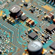
IoT devices are often deployed in environments where frequent battery replacement is impractical or impossible. Smart sensors in industrial facilities, wearable health monitors, and environmental monitoring systems may need to operate for months or even years on a single battery. A carefully designed System-on-a-Chip helps meet these requirements by consolidating multiple components into an energy-efficient architecture.

Traditional designs using separate microcontrollers, communication modules, and signal processors typically consume more power due to additional interfaces and data transfers. In contrast, a System on a Chip integrates these functions internally, reducing power loss and enabling optimized communication between subsystems.

Low-power System-on-a-Chip designs also enable developers to implement advanced energy-saving features such as dynamic voltage scaling, power gating, and multiple sleep modes. These capabilities allow devices to remain in ultra-low-power states when inactive while quickly waking to process data or transmit information when needed.

For battery-powered IoT devices, this level of efficiency can significantly extend operational lifespans. In applications like remote sensors or asset-tracking devices, an optimized System-on-a-Chip can be the difference between a device lasting several months and one lasting multiple years without maintenance.

Design Techniques for Maximizing Battery Life

Developing an ultra-efficient System-on-a-Chip for IoT applications requires careful design decisions and strategic trade-offs. Engineers must balance processing power, connectivity, and sensing capabilities with strict energy budgets.

One key design strategy is minimizing active processing time. Many IoT devices operate intermittently, waking only to collect sensor data or transmit updates. A System-on-a-Chip optimized for fast wake-up times and efficient task execution can complete these operations quickly before returning to a low-power sleep state.

Another important approach involves selecting the appropriate communication technology. Wireless protocols such as Bluetooth Low Energy, sub-GHz RF, and other low-power connectivity standards can significantly reduce energy consumption. Integrating these communication modules directly into the System-on-a-Chip helps eliminate external components and further improves power efficiency.

Analog front-end optimization is another critical factor. Sensors often generate weak signals that require amplification and filtering before processing. By integrating these functions directly into the System-on-a-Chip, designers can reduce noise, improve signal quality, and minimize power consumption.

Memory architecture also plays a role in power management. Designers often choose low-power SRAM or non-volatile memory technologies that offer fast access while consuming minimal energy. Efficient data management within the System-on-a-Chip helps ensure that the device performs necessary computations without wasting valuable battery power.

Enabling the Future of Connected Devices

As IoT adoption accelerates, the demand for energy-efficient semiconductor solutions will only increase. The System-on-a-Chip will remain a fundamental technology enabling the next generation of smart, connected devices.

By combining ultra-low-power design techniques with advanced integration capabilities, modern System-on-a-Chip architectures allow engineers to build IoT devices that are smaller, more capable, and significantly more energy-efficient. From smart healthcare wearables to industrial monitoring systems and environmental sensors, these solutions are powering a new era of intelligent, battery-powered technology.

Learn about our work at Linear MicroSystems by clicking here!


Linear MicroSystems, Inc. is proud to offer its services worldwide as well as the surrounding areas and cities around our Headquarters in Irvine, CA: Mission Viejo, Laguna Niguel, Huntington Beach, Santa Ana, Fountain Valley, Anaheim, Orange County, Fullerton, and Los Angeles.

Analog Design

Sensor ASICs in Healthcare: Revolutionizing Diagnostics and Patient Monitoring

Healthcare technology is evolving rapidly, driven by the need for more accurate diagnostics, real-time patient monitoring, and compact medical devices. At the heart of many of these innovations is the Sensor ASIC. Sensor ASIC enables medical devices to collect and analyze biological data with exceptional precision. As healthcare systems increasingly rely on data-driven insights, this technology is becoming a cornerstone of modern medical diagnostics and monitoring solutions.

The Role of Sensor ASIC Technology in Medical Devices

A Sensor ASIC is a custom integrated circuit designed to interface directly with sensors, process analog signals, and convert them into usable digital data. In healthcare applications, this capability is essential for transforming raw biological signals into actionable insights. Devices such as wearable monitors, implantable sensors, and portable diagnostic equipment depend on Sensor ASICs to operate efficiently and reliably.

One major advantage of a Sensor ASIC is its ability to integrate multiple functions onto a single chip. Instead of relying on separate components for signal amplification, filtering, and data conversion, a Sensor ASIC can perform these tasks internally. This integration reduces power consumption, minimizes device size, and improves overall reliability. For medical devices that must operate continuously or be worn by patients for extended periods, these benefits are critical.

Sensor ASIC solutions are commonly used in devices that measure vital physiological signals. By delivering highly accurate signal processing, a Sensor ASIC ensures that healthcare providers receive reliable data for diagnosis and treatment decisions. In applications where patient safety and data accuracy are paramount, the performance of the Sensor ASIC directly impacts the effectiveness of the entire system.

Sensor ASICs Improving Diagnostics & Continuous Patient Monitoring

The rise of remote healthcare and wearable medical technology has created a growing demand for advanced sensor systems. A Sensor ASIC plays a vital role in enabling these innovations by supporting continuous monitoring in compact, energy-efficient devices. Wearable health trackers, smart patches, and implantable sensors rely on Sensor ASIC architectures to capture and process physiological signals in real time.

Continuous monitoring offers significant advantages for both patients and clinicians. Instead of relying solely on periodic checkups, healthcare providers can observe trends in patient data over time. A Sensor ASIC allows these devices to gather high-resolution data while maintaining low power consumption, making long-term monitoring practical.

For example, cardiac monitoring devices equipped with a Sensor ASIC can detect subtle irregularities in heart rhythms. This can enable earlier intervention for conditions such as arrhythmias. Similarly, glucose monitoring systems benefit from Sensor ASIC integration, which provides consistent, real-time measurements that help patients manage chronic conditions more effectively.

Another key benefit of Sensor ASIC technology is improved diagnostic accuracy. Because the chip is custom-designed for a specific sensor and application, engineers can optimize signal conditioning and noise reduction. This leads to clearer data and more precise measurements, which ultimately enhances clinical decision-making.

The Future of Sensor ASIC Innovation in Healthcare

As medical devices become smaller, smarter, and more connected, the importance of the Sensor ASIC will continue to grow. Advances in semiconductor technology are enabling more sophisticated Sensor ASIC designs that incorporate artificial intelligence, wireless communication, and advanced data processing.

In the future, Sensor ASIC solutions will support next-generation healthcare applications such as personalized medicine, remote diagnostics, and advanced implantable devices. The way healthcare providers monitor, diagnose, and treat is transforming through accurate sensing and efficient data processing in compact systems. As innovation continues, this technology will remain a key driver of progress in modern medical electronics.

Learn about our work at Linear MicroSystems by clicking here!


Linear MicroSystems, Inc. is proud to offer its services worldwide as well as the surrounding areas and cities around our Headquarters in Irvine, CA: Mission Viejo, Laguna Niguel, Huntington Beach, Santa Ana, Fountain Valley, Anaheim, Orange County, Fullerton, and Los Angeles.

Analog Design

ASIC Cards for Ethereum Mining: A Comprehensive Guide

Cryptocurrency mining has evolved significantly over the past decade, with specialized hardware transforming how digital assets are produced. Among the most powerful tools developed for this purpose is the ASIC Card. For miners interested in maximizing efficiency and performance, understanding how an ASIC Card works and has been used in networks like Ethereum is essential. While the cryptocurrency mining landscape continues to evolve, the technology behind ASIC-based solutions remains a cornerstone of high-performance blockchain processing.

What Is an ASIC Card?

An ASIC Card is a hardware component built to execute a single type of computation extremely efficiently. Unlike general-purpose GPUs or CPUs, which are designed to handle a wide range of tasks, an ASIC Card is engineered to perform a specific algorithm or set of operations with maximum speed and minimal power consumption.

In cryptocurrency mining, this specialization offers a major advantage. Mining involves solving complex cryptographic puzzles that validate transactions and secure blockchain networks. An ASIC Card is designed specifically for these types of calculations, so it can perform them far faster than traditional hardware.

The structure of an ASIC Card typically includes custom silicon designed for hashing algorithms, integrated power management, and optimized communication with host systems. This allows the ASIC Card to deliver high hash rates while maintaining relatively low energy usage compared to general-purpose computing hardware.

For companies developing semiconductor solutions, designing an ASIC Card requires deep expertise in circuit architecture, signal optimization, and thermal efficiency. These factors are critical to ensuring reliable, long-term performance in demanding computational environments.

The Role of ASIC Cards in Cryptocurrency Mining

In early cryptocurrency mining, individuals commonly used CPUs and later GPUs to process transactions and earn rewards. As mining difficulty increased and competition grew, specialized hardware quickly became necessary. This is where the ASIC Card emerged as a dominant solution.

By focusing exclusively on the mathematical functions used in mining algorithms, an ASIC Card can dramatically outperform traditional hardware. This performance advantage allows miners to process more transactions, verify more blocks, and increase potential rewards.

Historically, some cryptocurrency networks explored ASIC-compatible mining approaches to improve processing efficiency. The use of an ASIC Card allowed large-scale mining operations to optimize both performance and energy consumption. These are two of the most important factors for profitability.

Beyond raw performance, another key benefit of an ASIC Card is scalability. Mining operations can deploy multiple ASIC Cards in parallel, building large computational clusters capable of handling enormous workloads. These systems often rely on advanced cooling solutions and optimized power distribution to maintain stable operation under continuous load.

For semiconductor developers, designing an ASIC Card for mining requires balancing computational throughput with energy efficiency. Even small improvements in power efficiency can translate into significant cost savings when thousands of cards are deployed in large mining facilities.

Future Considerations for ASIC Card Development

As blockchain technologies continue to mature, the demand for specialized hardware remains strong. While some networks have transitioned away from traditional mining methods, the design principles behind the ASIC Card continue to influence high-performance computing solutions used across the broader cryptocurrency ecosystem.

For microsystems and semiconductor companies, ASIC Card development represents an opportunity to push the boundaries of custom silicon design. Advances in chip architecture, energy efficiency, and system integration will continue to shape the next generation of specialized computing hardware.

Ultimately, the ASIC Card demonstrates the power of application-specific design. By tailoring hardware to the precise needs of complex computational tasks, engineers can achieve performance and efficiency levels that general-purpose processors simply cannot match.

Learn about our work at Linear MicroSystems by clicking here!


Linear MicroSystems, Inc. is proud to offer its services worldwide as well as the surrounding areas and cities around our Headquarters in Irvine, CA: Mission Viejo, Laguna Niguel, Huntington Beach, Santa Ana, Fountain Valley, Anaheim, Orange County, Fullerton, and Los Angeles.

SOC

System on a Chip Solutions Driving Advances in Aerospace and Defense Technology

Aerospace and defense systems demand exceptional performance, reliability, and efficiency in some of the world’s most challenging environments. From extreme temperatures and radiation exposure to strict size, weight, and power constraints, electronic systems must meet uncompromising standards. In this landscape, SOC (System on a Chip) solutions have emerged as a critical enabler, integrating complex functionality into compact, high-performance semiconductor platforms that support next-generation aerospace and defense applications.

The Role of SOC Integration in Mission-Critical Systems

Traditional aerospace and defense electronics relied on multiple discrete components spread across large circuit boards. While effective, these architectures increased system weight, power consumption, and points of failure. SOC solutions transform this approach by integrating processors, memory, interfaces, analog blocks, and security features onto a single chip.

This high level of integration delivers several advantages. First, SOC architectures significantly reduce size and weight, key factors in aircraft, satellites, unmanned aerial vehicles (UAVs), and missile systems. Second, shorter interconnects improve signal integrity and performance while lowering power consumption. Finally, fewer components translate to higher system reliability, a non-negotiable requirement in mission-critical defense environments.

By consolidating diverse functions into a unified design, SOC platforms enable faster data processing, real-time decision-making, and seamless communication between subsystems.

Enabling Advanced Capabilities Through SOC Design

Modern aerospace and defense platforms increasingly rely on sophisticated technologies, including radar, electronic warfare, secure communications, and autonomous navigation. SOC solutions play a central role in enabling these capabilities by supporting high-speed data acquisition, processing, and control within a single silicon device.

For example, advanced SOC designs can integrate digital signal processors, high-performance CPUs, and hardware accelerators to handle complex algorithms for target detection, tracking, and threat analysis. Embedded analog and mixed-signal blocks allow SOC devices to interface directly with sensors, antennas, and actuators, reducing latency and improving system responsiveness.

Security is another critical area where SOC technology excels. Defense systems require robust protection against tampering, cyber threats, and data breaches. SOC platforms can embed hardware-based security features, such as encryption engines, secure boot mechanisms, and trusted execution environments, thereby ensuring that sensitive information remains protected throughout the system lifecycle.

Meeting Harsh Environment and Long-Lifecycle Requirements

Aerospace and defense applications often operate in harsh conditions, including high radiation levels, extreme temperatures, and mechanical stress. SOC solutions designed for these environments incorporate specialized process technologies, redundancy techniques, and fault-tolerant architectures to maintain reliable operation over long mission lifespans.

In addition, defense programs typically require long product lifecycles and consistent performance over decades. SOC designs can be tailored to meet these requirements through rigorous qualification, controlled manufacturing processes, and support for legacy interfaces alongside modern technologies.

The Future of SOC in Aerospace and Defense

As aerospace and defense systems continue to evolve, the importance of SOC solutions will only grow. Increasing autonomy, higher data rates, and tighter power budgets demand even greater integration and efficiency. By delivering scalable, secure, and high-performance platforms, SOC technology is driving innovation across aerospace and defense, enabling smarter, lighter, and more capable systems for tomorrow’s missions.

Learn about our work at Linear MicroSystems by clicking here!


Linear MicroSystems, Inc. is proud to offer its services worldwide as well as the surrounding areas and cities around our Headquarters in Irvine, CA: Mission Viejo, Laguna Niguel, Huntington Beach, Santa Ana, Fountain Valley, Anaheim, Orange County, Fullerton, and Los Angeles.

Mixed Signal ASIC Design

How to Optimize Power Efficiency in Mixed Signal ASIC Design

Power efficiency has become a defining requirement in modern semiconductor development. As devices shrink, become more intelligent, and become more interconnected, designers must deliver high performance while minimizing energy consumption. This challenge is especially critical in Mixed Signal ASIC Design, where analog and digital circuits coexist on the same chip and compete for power, area, and signal integrity. Optimizing power efficiency requires a holistic approach that spans architecture, circuit design, and system-level considerations.

Understanding Power Challenges in Mixed Signal ASIC Design

Mixed Signal ASIC Design presents unique power challenges because analog and digital blocks behave very differently. Digital circuits primarily consume dynamic power from switching activity, whereas analog circuits often require constant bias currents to maintain accuracy and stability. When combined on a single die, these blocks can introduce noise, leakage, and thermal issues that negatively impact overall efficiency.

Additionally, many applications, such as IoT devices, medical equipment, and automotive electronics, operate under strict power budgets. In these environments, inefficient power management can reduce battery life, limit performance, or increase system cost. As a result, power optimization must be addressed early in the Mixed Signal ASIC Design process rather than treated as a late-stage refinement.

Architectural Strategies for Power Optimization

One of the most effective ways to improve power efficiency in Mixed Signal ASIC Design is through thoughtful system architecture. Partitioning the design into multiple power domains allows individual blocks to be powered up or down as needed. Power gating techniques can significantly reduce leakage by shutting off inactive sections of the chip, particularly in digital logic.

Clock management is another critical strategy. Reducing clock frequency, implementing clock gating, and minimizing unnecessary switching activity can dramatically lower dynamic power consumption. On the analog side, designers can select architectures that meet performance targets with lower bias currents, such as current-efficient amplifiers or low-power data-converter topologies.

Voltage scaling also plays a key role. Operating digital circuits at the lowest possible supply voltage reduces power quadratically, while careful analog design ensures performance is maintained despite reduced voltage headroom. Balancing these trade-offs is a central challenge in power-aware Mixed Signal ASIC Design.

Circuit-Level Techniques and Design Trade-Offs

At the circuit level, optimizing power efficiency requires careful component selection and biasing. In analog blocks, techniques such as adaptive biasing allow circuits to draw more current only when higher performance is required. This dynamic behavior improves efficiency without sacrificing accuracy during critical operating conditions.

For digital circuits, minimizing transistor sizes where possible reduces capacitance and switching power. Designers must also account for leakage currents, which become more significant in advanced process nodes. Choosing appropriate threshold voltages and optimizing sleep modes can help mitigate these losses.

Equally important is managing the interaction between analog and digital domains. Proper isolation, grounding strategies, and layout techniques prevent digital switching noise from forcing analog circuits to consume extra power to maintain performance.

Designing for Power-Aware Applications

Ultimately, successful power optimization in Mixed Signal ASIC Design depends on aligning design choices with real-world application requirements. Whether the goal is to extend battery life, reduce thermal output, or meet regulatory efficiency standards, power must be treated as a first-class design metric.

By combining smart architecture, efficient circuit techniques, and system-level awareness, microsystem companies can deliver Mixed Signal ASIC solutions that achieve optimal power efficiency without compromising functionality or reliability.

Learn about our work at Linear MicroSystems by clicking here!


Linear MicroSystems, Inc. is proud to offer its services worldwide as well as the surrounding areas and cities around our Headquarters in Irvine, CA: Mission Viejo, Laguna Niguel, Huntington Beach, Santa Ana, Fountain Valley, Anaheim, Orange County, Fullerton, and Los Angeles.

Analog Design

The Evolution of Analog Design: From Simple Circuits to Complex Systems

Analog Design has been a foundational element of electronics since the earliest days of electrical engineering. Long before digital systems dominated the technology landscape, analog circuits were responsible for amplifying signals, regulating power, and enabling communication across vast distances. Over time, Analog Design has evolved dramatically, shifting from simple, discrete components to highly integrated solutions that power today’s complex semiconductor systems. Understanding this evolution offers valuable insight into why analog expertise remains essential in modern microsystems.

Early Foundations of Analog Design

The origins of Analog Design date back to the late 19th and early 20th centuries, when engineers relied on basic components such as resistors, capacitors, inductors, and vacuum tubes. Early analog circuits were used in radios, telephones, and early power systems, where continuous electrical signals represented sound, light, or motion. These designs were largely handcrafted, requiring deep intuition and hands-on experimentation.

The invention of the transistor in the late 1940s marked a turning point for Analog Design. Transistors replaced bulky vacuum tubes, enabling smaller, more reliable, and more energy-efficient circuits. During this era, analog engineers focused on amplifiers, oscillators, and filters that formed the backbone of early consumer electronics and industrial control systems. Despite their relative simplicity, these circuits required precision, as small variations in component values could significantly affect performance.

The Rise of Integrated Circuits and Mixed-Signal Systems

As semiconductor manufacturing advanced in the 1960s and 1970s, Analog Design entered a new phase with the introduction of integrated circuits (ICs). Instead of assembling discrete components, engineers could now integrate multiple analog functions onto a single chip. This innovation improved consistency, reduced cost, and enabled entirely new applications.

With the growth of digital computing, Analog Design did not disappear; instead, it became more critical. Modern systems rely on mixed-signal designs that combine analog and digital circuitry on the same silicon. Analog circuits handle real-world signals such as voltage, current, temperature, and radio-frequency signals, while digital logic processes and interprets data. Designing these systems requires balancing noise, power efficiency, and signal integrity, making Analog Design more complex and specialized than ever before.

Modern Applications in Complex Semiconductor Systems

Today, Analog Design plays a vital role in advanced microsystems across industries such as automotive, medical devices, telecommunications, and renewable energy. High-performance analog blocks are essential for sensors, data converters, power management ICs, and RF communication systems. As semiconductor nodes shrink and systems become more integrated, analog engineers face challenges such as reduced voltage headroom, increased interference, and stricter performance requirements.

Despite these challenges, Analog Design continues to evolve through innovative architectures, advanced simulation tools, and close collaboration between design and process engineering teams. In an increasingly digital world, analog circuits remain the critical bridge between physical phenomena and digital intelligence.

Looking Ahead

The evolution of Analog Design reflects the broader history of electronics, one of constant adaptation and innovation. From simple circuits built with discrete components to sophisticated systems-on-chip, analog engineering remains indispensable. As microsystems grow more complex, the demand for skilled Analog Design will continue to rise, ensuring its continued relevance.

Learn about our work at Linear MicroSystems by clicking here!


Linear MicroSystems, Inc. is proud to offer its services worldwide as well as the surrounding areas and cities around our Headquarters in Irvine, CA: Mission Viejo, Laguna Niguel, Huntington Beach, Santa Ana, Fountain Valley, Anaheim, Orange County, Fullerton, and Los Angeles.

Sensor ASICs

The AI Acceleration Revolution: Why ASICs are the Unsung Heroes of Edge AI

Artificial intelligence is rapidly moving from centralized cloud environments to the edge, closer to where data is generated. From smart cameras and industrial robots to medical devices and autonomous systems, edge AI enables real-time decision-making with lower latency, improved reliability, and enhanced data privacy. At the center of this transformation lies a critical but often overlooked technology: the Sensor ASIC. While GPUs and general-purpose processors receive much of the attention, custom ASICs are quietly powering the next generation of edge AI applications.

Why Edge AI Demands Specialized Hardware

Edge AI systems face unique constraints that traditional computing architectures struggle to meet. Limited power budgets, compact form factors, and real-time processing requirements demand hardware that is both highly efficient and purpose-built. Unlike cloud-based AI, edge devices cannot rely on vast compute resources or continuous connectivity.

This is where the Sensor ASIC plays a pivotal role. By integrating sensor interfaces, signal processing, and AI acceleration into a single chip, Sensor ASICs dramatically reduce data movement and processing overhead. Instead of sending raw sensor data to external processors or the cloud, intelligence is embedded directly at the point of capture. This localized processing improves responsiveness while minimizing energy consumption, an essential requirement for battery-powered and always-on edge devices.

Sensor ASICs as AI Accelerators

A Sensor ASIC is uniquely positioned to accelerate AI workloads at the edge because it is designed around the specific characteristics of the sensor and application. Whether handling vision data, LiDAR signals, or biomedical measurements, Sensor ASICs can incorporate custom data paths, hardware accelerators, and memory architectures optimized for machine learning inference.

By eliminating unnecessary general-purpose logic, Sensor ASICs deliver significantly higher performance per watt than CPUs or GPUs. This efficiency enables real-time AI inference, such as object detection or anomaly recognition, without the thermal and power penalties associated with more flexible computing platforms. As a result, edge AI systems can scale in complexity while remaining within strict power and size constraints.

Enabling Smarter, More Reliable Edge Systems

Beyond performance and efficiency, Sensor ASICs enhance system reliability and determinism, key factors in safety-critical applications. In automotive, industrial automation, and healthcare, predictable response times and robust operation are non-negotiable. Custom ASICs provide deterministic processing behavior that software-driven systems often struggle to guarantee.

Additionally, Sensor ASICs enable tighter integration of security features directly into hardware. Secure boot, encrypted data paths, and tamper resistance can be embedded at the silicon level, protecting sensitive sensor data and AI models from unauthorized access. This is increasingly important as edge devices become targets for cyber threats.

Market Momentum and Future Outlook

The growing adoption of edge AI is accelerating demand for Sensor ASIC solutions across industries. Smart infrastructure, autonomous machines, and next-generation medical devices all require intelligent sensing with minimal latency and power draw. As AI models become more efficient and specialized, the value of hardware tailored to specific sensing and inference tasks continues to rise.

Looking ahead, Sensor ASICs will be central to enabling scalable, cost-effective edge AI deployments. Their ability to combine sensing, processing, and intelligence on a single chip makes them indispensable to the AI acceleration revolution.

Sensor ASICs Conclusion

The Sensor ASIC is a foundational technology driving the success of edge AI. By delivering unmatched efficiency, performance, and integration, ASICs empower intelligent systems to operate where they matter most. For companies shaping the future of AI-enabled devices, Sensor ASICs are the unsung heroes enabling edge intelligence.


Linear MicroSystems, Inc. is proud to offer its services worldwide as well as the surrounding areas and cities around our Headquarters in Irvine, CA: Mission Viejo, Laguna Niguel, Huntington Beach, Santa Ana, Fountain Valley, Anaheim, Orange County, Fullerton, and Los Angeles.

Mixed Signal ASIC Design

The Economics of 3D Imaging ASICs

As industries from automotive to aerospace increasingly demand high-performance, power-efficient imaging solutions, the adoption of 3D Imaging ASIC technology is gaining momentum. Unlike general-purpose imaging hardware, 3D imaging is designed to handle depth sensing, point cloud processing, and advanced vision algorithms with optimized efficiency. Yet the economics of these custom silicon solutions can be complex. Understanding the cost structures, ROI, and evolving market trends is essential for companies considering entry into this space.

Cost Considerations in 3D Imaging ASIC Development

At the core of any 3D Imaging ASIC project is the initial investment required for design and fabrication. Custom ASIC development entails significant upfront engineering effort, including hardware design, verification, simulation, and software integration. These engineering costs are amplified by the need for deep expertise in analog/digital integration, sensor interfaces, and power management specific to 3D imaging workloads.

Fabrication expenses also play a major role. Advanced process nodes that deliver high performance and low power consumption are expensive, and mask sets for custom silicon can cost millions. Even with multi-project wafer sharing and prototype runs, the non-recurring engineering charges for ASICs remain substantial.

However, unlike FPGAs or off-the-shelf processors, 3D Imaging offers optimized cost per unit when deployed at scale. Once the design and masks are amortized across large production volumes, the per-chip cost becomes highly competitive. This shift in unit economics is often a tipping point for commercialization. Especially so in markets such as consumer electronics and automotive, where millions of units may be deployed.

Return on Investment: Beyond Unit Costs

Evaluating the ROI of a 3D Imaging ASIC project requires looking beyond simple unit economics to include performance, power efficiency, and differentiation value. Custom ASICs deliver higher performance and lower energy consumption than general-purpose processors and FPGAs because they eliminate unnecessary logic and tailor resources to specific tasks, such as depth calculation or 3D reconstruction.

For end-product manufacturers, this performance advantage can translate into tangible benefits: longer battery life in portable devices, real-time sensing in autonomous vehicles, and improved accuracy in medical imaging systems. These competitive advantages can justify higher product pricing and foster stronger brand positioning, enhancing overall ROI.

Moreover, the marketplace is increasingly valuing customized silicon as a catalyst for innovation. Companies that integrate 3D Imaging ASIC technology can offer differentiated features. These include advanced gesture recognition or precise spatial mapping, which are difficult to replicate with generic hardware. This innovation premium drives long-term revenue growth and customer loyalty.

Market Trends Driving Adoption

Several macroeconomic trends are accelerating the adoption of 3D Imaging ASICs. Demand for ADAS Autonomous vehicles has sparked interest in robust, low-latency 3D perception solutions. Similarly, robotics, AR, and industrial automation are driving the need for compact, power-efficient 3D vision systems.

At the same time, supply chain dynamics and the push for domestic semiconductor capability are influencing investment decisions. Organizations increasingly view custom ASICs as strategic assets rather than discretionary projects. Especially so, where security, performance, and long-term cost efficiency are priorities.

Strategic Takeaways for Businesses

The economics of 3D Imaging ASICs ultimately balance high upfront investment against scalable unit costs, strategic performance advantages, and market demand. Companies that thoughtfully plan design, production, and product integration can unlock compelling long-term value. For businesses evaluating 3D imaging solutions, a deep understanding of these economic drivers is critical for informed decision-making in an increasingly competitive semiconductor landscape.

Interested in 3d Imaging ASICs for your next project? Click here to contact Linear MicroSystems!


Linear MicroSystems, Inc. is proud to offer its services worldwide as well as the surrounding areas and cities around our Headquarters in Irvine, CA: Mission Viejo, Laguna Niguel, Huntington Beach, Santa Ana, Fountain Valley, Anaheim, Orange County, Fullerton, and Los Angeles.

System-on-a-chip

Top Benefits of Custom System on a Chip Design for Modern Applications

As electronic systems become smaller, faster, and more intelligent, companies across industries are turning to custom System-on-a-Chip (SoC) designs to meet increasingly complex performance and integration demands. From medical devices and industrial automation to aerospace and consumer electronics, custom SoC solutions offer a level of efficiency and control that off-the-shelf components cannot match. For organizations developing next-generation products, investing in a custom System-on-a-Chip architecture can provide a decisive competitive advantage.

Higher Performance Through Optimized Integration

One of the most significant benefits of custom System-on-a-Chip design is the ability to integrate multiple system components onto a single silicon die. Processing cores, memory blocks, analog interfaces, communication modules, and accelerators can be designed to work together seamlessly. This high level of integration reduces latency, improves data throughput, and enables faster real-time processing.

Unlike general-purpose chips, a custom System-on-a-Chip is optimized for specific application requirements. Designers can tailor processing power, clock speeds, and data paths to meet exact performance targets. This is especially valuable in applications such as edge computing, medical imaging, and autonomous systems, where responsiveness and reliability are critical.

Reduced Power Consumption and Improved Efficiency

Power efficiency is a significant concern in modern electronics, particularly for battery-powered and embedded systems. Custom System-on-a-Chip designs allow engineers to minimize power consumption by eliminating unnecessary circuitry and optimizing voltage domains. By integrating only the functions required for a specific application, SoC designs reduce energy waste and extend device operating life.

Advanced power management features such as dynamic voltage scaling, power gating, and sleep modes can be embedded directly into the System-on-a-Chip architecture. This level of control is difficult to achieve with discrete components and is essential for applications in wearables, portable medical devices, and remote sensors.

Smaller Form Factors and Lower System Costs

As devices continue to shrink, space constraints become more challenging. A custom System-on-a-Chip dramatically reduces board size by consolidating multiple components into a single chip. This enables smaller, lighter, and more compact product designs without sacrificing functionality.

In addition to saving space, a System-on-a-Chip can reduce overall system costs over time. While the initial development investment may be higher, integrating components lowers bill-of-materials costs, simplifies assembly, and improves manufacturing yields at scale. For high-volume applications, these efficiencies translate into significant long-term savings.

Enhanced Security and Reliability

Custom System-on-a-Chip solutions also offer improved security and system reliability. Hardware-based security features such as secure boot, encryption engines, and trusted execution environments can be built directly into the chip. This is particularly important for applications that handle sensitive data or operate in regulated industries.

By reducing interconnects and external components, a System-on-a-Chip design also minimizes potential points of failure. Fewer connections mean improved signal integrity and higher overall system reliability, which is critical in mission- and safety-critical applications.

Enabling Innovation Across Modern Applications

Custom System-on-a-Chip design empowers companies to innovate faster and differentiate their products in competitive markets. With greater control over performance, power, size, and security, SoC solutions provide a scalable foundation for modern applications across healthcare, industrial, automotive, and beyond.

For microsystems companies developing advanced technologies, custom System-on-a-Chip architectures are not just an engineering choice; they are a strategic investment in long-term product success.

Click here to contact a Linear MicroSystems expert today!


Linear MicroSystems, Inc. is proud to offer its services worldwide as well as the surrounding areas and cities around our Headquarters in Irvine, CA: Mission Viejo, Laguna Niguel, Huntington Beach, Santa Ana, Fountain Valley, Anaheim, Orange County, Fullerton, and Los Angeles.

Mixed Signal ASIC Design

ASIC Card Security: How to Protect Your Investment

From medical devices to aerospace to advanced robotics, protecting the technology behind these systems is more critical than ever. An ASIC Card represents a significant investment in performance, efficiency, and competitive differentiation. Ensuring these cards remain secure throughout their lifecycle is essential to safeguard intellectual property, prevent system failures, and maintain long-term operational integrity.

Why ASIC Card Security Matters

Unlike off-the-shelf components, an ASIC Card is built with proprietary architectures and features tailored to a company’s product or application. This makes it a valuable target for industrial espionage, counterfeiting, and tampering as embedded systems become more connected and data-driven; security risks increase not just from physical access but also from cyberattacks and unauthorized system integrations.

Hardware-level threats can disrupt system performance, compromise sensitive data, or reverse-engineer proprietary circuitry. In industries such as defense, medical imaging, and industrial automation, these risks can lead to far more than financial losses; they may impact safety, compliance, and mission-critical operations.

Building strong security into an ASIC Card from the design phase helps ensure durability against emerging threats and extends the device’s operational life.

Best Practices for Protecting Your ASIC Investment

Protecting an ASIC Card requires a multi-layered security strategy that includes both physical and digital safeguards. The following practices help maintain security throughout deployment, maintenance, and the device’s full lifecycle.

1. Hardware-Embedded Security Features
Hardware-embedded security is he most effective protection that begins at the silicon level. Integrating features such as secure boot, hardware encryption modules, unique chip identifiers, and tamper-detection circuits prevents unauthorized access and ensures only trusted firmware can be executed.

Secure boot ensures that any software running on the ASIC Card is verified, preventing malicious updates or code injections.

2. Physical Tamper Resistance
In environments where hardware may be physically accessed, tamper-resistant packaging and sensors can detect attempts to probe or disassemble the hardware. This helps protect intellectual property, especially in high-risk industries such as aerospace and advanced manufacturing.

Coatings, epoxy encapsulation, and secure enclosures add layers of defense against physical intrusion and reverse engineering.

3. Firmware and Software Protection
While ASICs are primarily hardware-based, firmware still plays a vital role. Access control, encrypted firmware updates, and secure communication protocols ensure that no unauthorized party can modify the system.

Regular patching and cryptographic signing further safeguard firmware from exploitation.

4. Lifecycle and Supply Chain Security
Securing an ASIC Card extends beyond deployment. Counterfeit prevention, secure manufacturing processes, and traceability throughout the supply chain ensure that only authorized components enter your ecosystem.

Post-deployment monitoring and authenticated servicing help maintain security as systems age.

Protecting Your Competitive Edge

With increasing reliance on specialized silicon, securing your ASIC Card is no longer optional; it’s essential to protecting your intellectual property, product performance, and customer trust. By integrating strong security measures into your design, manufacturing, and lifecycle management processes, you ensure that your investment continues delivering value for years to come.


Linear MicroSystems, Inc. is proud to offer its services worldwide as well as the surrounding areas and cities around our Headquarters in Irvine, CA: Mission Viejo, Laguna Niguel, Huntington Beach, Santa Ana, Fountain Valley, Anaheim, Orange County, Fullerton, and Los Angeles.