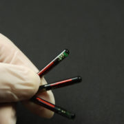
ASIC Chip Design Flow
Engineers must mimic a tried-and-tested ASIC chip design flow to guarantee successful ASIC design. This should be derived from having a good understanding of ASIC specifications, low power design, and performance, requirements while focusing on achieving the goal of the right time to market.
So, what are we talking about?
- Design specification
- Architectural design
- Behavioral and functional modeling
- Logical implementation
- Synthesis and testing
- Place and route
- Design layout
The ASIC chip design cycle
Certainly, fulfilling the demands of ASIC chip design is achievable by applying changes in design tools, methodologies, and hardware and software capabilities.
So, what do you need to know?
Chip specification
- This is the time when the engineer will define features, functionalities, microarchitecture, and specifications with design guidelines of the ASIC chip. So, there are two teams involved, namely the design team and the verification team.
Design entry / functional verification
- This confirms the functionality and logical behavior of the circuit by simulation on the design entry level. Then, the design and verification teams will come into play at this stage to generate RTL code with the use of test benches. This process is the behavioral simulation.
-
-
Types of simulation tools
-
-
-
- Functional simulation tools – This will verify logical behavior. Also, the implementation after the testbench and design code.
- Timing simulation tools – This will verify the timing requirements are in check by the circuit design. Also, will confirm the design is free of delays in the circuit signal.
-
RTL block synthesis / RTL function
- After the generation of RTL code and testbench, the RTL team will work on the description by translating the RTL code into a gate-level netlist with the use of a logical synthesis tool.
Chip partitioning
- This is when the engineer follows the ASIC design layout requirement and specification for the creation of its structure aided by EDA tools with proven methodologies.
Design for test insertion
- To ensure that system-on-chip variation requirements are in check, new models and techniques allow for high-quality testing. Thus, the design for the test comes with a number of techniques.
Scan path insertion
-
- This links all register elements into a single long shift register to evaluate small parts of the design instead of the entire design in a single process.
Memory built-in self-test
-
- Certainly, chip memory requires lower area and fast access time in lower technology nodes. So, the memory built-in self-test is a device that checks RAMs.
Automatic test pattern generation
-
- This method creates test vectors or sequential input patterns to check for faults in different elements of a circuit.
Floorplanning
- This is the first step in RTL-to-GDSII design, which places blocks into chips. In any case, the floorplan will determine the size of the chip and places the gates and connects them with wires.
Placement
- This process is the placement of standard cells in a row.
Clock tree synthesis
- This process builds the clock tree. Also, meets the defined timing, area, and power requirements.
Routing
- This process is done via global and detailed routing.
Global routing
-
- This calculates estimated values per net by the delays of wire fanout.
Detailed routing
-
- This is where the actual delays of wire are calculated by different methods. So, among others, these methods are timing optimization and clock tree synthesis.
Final verification
- This process involves 3 steps of physical verification also known as signoff checks. Also, this will help check if the layout is working just as it intends to.
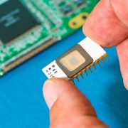
GDS II or graphical data stream information interchange
- The engineer will perform wafer processing, packaging, testing, verification, and delivery to the physical IC in this final step.
Interested in getting your next project going with our experts at Linear MicroSystems? Click here to go to our contact page!
Linear MicroSystems, Inc. is proud to offer its services worldwide as well as the surrounding areas and cities around our Headquarters in Irvine, CA: Mission Viejo, Laguna Niguel, Huntington Beach, Santa Ana, Fountain Valley, Anaheim, Orange County, Fullerton, and Los Angeles.