Exploring the Role of SoC in Edge Computing: Enhancing Performance and Efficiency
System-on-a-chip (SoC) technology has become a pivotal player in edge computing, where processing power and efficiency are paramount. SoC integrates various components of a computer or other electronic systems into a single integrated circuit, offering a compact, energy-efficient solution for edge computing applications. This article delves into the significance of SoC in edge computing, highlighting its role in enhancing performance and efficiency.
Understanding SoC: A Comprehensive Solution
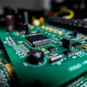
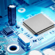
SoC is a revolutionary approach to hardware design that consolidates multiple functionalities onto a single chip. Traditionally, computing systems relied on separate components such as CPUs, GPUs, memory modules, and peripheral interfaces, each performing specific tasks. However, SoC combines these components into a cohesive unit, streamlining the overall architecture and reducing power consumption.
SoC’s heart lies in its ability to integrate diverse components onto a single chip, including processors, memory, I/O interfaces, and specialized accelerators. This integration reduces the device’s physical footprint and minimizes latency by reducing the distance data needs to travel between components. As a result, SoC offers a compelling solution for edge computing applications where space, power, and performance are critical factors.
Enhancing Performance and Efficiency at the Edge
Edge computing brings processing power closer to the data source, enabling real-time analytics, rapid decision-making, and low-latency responses. SoC plays a pivotal role in enhancing the performance and efficiency of edge computing devices by delivering powerful processing capabilities in a compact form factor.
One of the key advantages of SoC in edge computing is its ability to optimize power consumption without compromising performance. These devices can deliver high-performance computing while minimizing energy consumption by integrating power-efficient processors and specialized accelerators tailored for edge workloads. This is particularly crucial in edge environments where power constraints may limit the deployment of traditional computing systems.
Furthermore, SoC enables seamless integration with various sensors, actuators, and communication interfaces commonly found in edge devices. This integration facilitates efficient data collection, processing, and transmission, enabling edge devices to respond rapidly to changing conditions without relying on centralized data processing.
Driving Innovation in Edge Computing
As the demand for edge computing continues to surge across various industries, SoC technology is driving innovation by enabling new use cases and applications. From autonomous vehicles and industrial IoT to smart cities and healthcare systems, SoC-powered edge devices are revolutionizing how data is processed, analyzed, and acted upon at the network edge.
The versatility allows for customization and scalability, enabling developers to tailor edge computing solutions to meet specific requirements and constraints. Whether it’s deploying intelligent surveillance cameras, monitoring equipment in remote locations, or enabling predictive maintenance in industrial settings, SoC empowers organizations to harness the full potential of edge computing.
In conclusion, this technology redefines the edge computing landscape by delivering unparalleled performance, efficiency, and flexibility. By integrating multiple components onto a single chip, SoC devices offer a compact, energy-efficient solution for edge computing applications. As the demand for edge computing grows, SoC will play an increasingly vital role in driving innovation and unlocking new possibilities across industries.
If you’re interested in leveraging SoC technology for your edge computing initiatives, contact us to learn more about our cutting-edge solutions and how they can help accelerate your journey toward digital transformation.
Linear MicroSystems, Inc. is proud to offer its services worldwide as well as the surrounding areas and cities around our Headquarters in Irvine, CA: Mission Viejo, Laguna Niguel, Huntington Beach, Santa Ana, Fountain Valley, Anaheim, Orange County, Fullerton, and Los Angeles.