The Advantages and Limitations of Microsystems
Microsystems have emerged as a groundbreaking technology, revolutionizing various industries with their compact size and powerful capabilities. This article explores the advantages and limitations of microsystems, shedding light on their impact in the realm of technology and innovation.
Advantages of Microsystems
Miniaturization and Portability
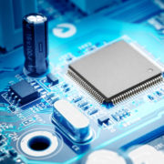
Microsystems owe their prominence to their miniature size, allowing for the integration of complex functionalities into small, portable devices. This miniaturization has paved the way for the development of ultra-compact sensors, actuators, and communication devices. As a result, industries such as healthcare, telecommunications, and consumer electronics have witnessed a surge in innovative applications. Wearable health monitors, tiny communication devices, and compact environmental sensors are just a few examples of how microsystems have transformed the way we interact with technology.
Energy Efficiency and Sustainability
One notable advantage lies in their energy efficiency. The reduced size of components often translates to lower power consumption, making microsystems an eco-friendly solution. This energy efficiency is particularly crucial in applications where battery life is a limiting factor. They contribute to the development of sustainable technologies, such as energy-efficient sensors for smart buildings, agricultural monitoring systems, and low-power medical implants.
Limitations of Microsystems
Integration Challenges
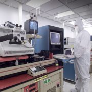
While microsystems offer compact solutions, their integration into larger systems can present challenges. Compatibility issues, standardization problems, and the need for specialized interfaces may arise when incorporating them into existing frameworks. Engineers and developers must navigate these complexities to ensure seamless integration, often requiring custom solutions and careful consideration of the overall system architecture.
Reliability and Durability Concerns
Microsystems, due to their size, may be more susceptible to environmental factors and mechanical stress. This vulnerability can impact their reliability and durability, especially in harsh conditions or high-stress applications. Manufacturers must address these concerns through rigorous testing and the implementation of protective measures to enhance their robustness. Balancing the quest for miniaturization with the need for resilience remains a constant challenge in the development of reliable microsystems.
Microsystems Conclusion
In conclusion, microsystems have undeniably transformed the technological landscape with their numerous advantages, ranging from miniaturization and portability to energy efficiency. However, like any technology, these come with a set of limitations, such as integration challenges and concerns about reliability and durability. As the field continues to evolve, addressing these limitations will be crucial for unlocking their full potential and ensuring their seamless integration into diverse applications. By understanding both the advantages and limitations, stakeholders in the industry can work towards pushing the boundaries of innovation and driving the next wave of technological advancements.
Looking for more information from the experts? Click here to visit our home page!
Linear MicroSystems, Inc. is proud to offer its services worldwide as well as the surrounding areas and cities around our Headquarters in Irvine, CA: Mission Viejo, Laguna Niguel, Huntington Beach, Santa Ana, Fountain Valley, Anaheim, Orange County, Fullerton, and Los Angeles.