Challenges of Lidar ASIC: Overcoming Obstacles
Lidar ASIC technology has become increasingly popular in the automotive industry for its ability to provide high-resolution imaging and mapping. Lidar, or Light Detection and Ranging, uses laser beams to measure the distance to objects in its field of view. However, the development of Lidar ASIC technology has faced several challenges, from cost to performance. In this article, we will explore some of the biggest hurdles in developing Lidar ASIC technology and discuss potential solutions and workarounds.
Cost of Lidar ASIC Technology
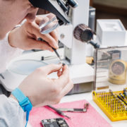
One of the biggest challenges in developing Lidar ASIC technology is the high cost of production. Lidar ASICs require advanced manufacturing processes and are typically produced in small volumes, which can drive up costs. The high cost of this technology has made it difficult for many companies to adopt the technology, particularly in the consumer market.
To overcome this challenge, companies are exploring different approaches to reduce the overall cost. One approach is to use lower-cost manufacturing processes, such as CMOS (Complementary Metal-Oxide-Semiconductor) technology, to produce Lidar ASICs. Another approach is to increase the volume of production, which can help drive down costs through economies of scale.
Performance of Lidar ASIC Technology
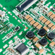
Another challenge in developing this technology is achieving the necessary performance for the intended application. For example, automotive Lidar ASICs must be able to provide high-resolution imaging and mapping in a variety of weather and lighting conditions.
To achieve the necessary performance, Lidar ASICs must have a high sampling rate and high signal-to-noise ratio. However, achieving high performance while keeping power consumption low is a major challenge. Power consumption is particularly important for automotive applications, where Lidar ASICs must operate in harsh environments while consuming minimal power.
To overcome this challenge, designers are exploring different approaches to optimize Lidar ASIC performance. One approach is to use advanced signal processing techniques to improve the signal-to-noise ratio of Lidar ASICs. Another approach is to optimize the power consumption of Lidar ASICs through the use of low-power design techniques.
Conclusion
The development of Lidar ASIC technology has faced several challenges, including high production costs and the need for high performance in harsh environments. However, by exploring different approaches to reduce costs and optimize performance, companies can overcome these challenges and bring Lidar ASIC technology to a wider range of applications. Lidar ASICs have the potential to revolutionize the automotive industry by providing high-resolution imaging and mapping, enabling safer and more efficient transportation. As Lidar ASIC technology continues to evolve, we can expect to see more innovative solutions that overcome these challenges and drive the adoption of this technology in a wider range of applications.
Linear MicroSystems, Inc. is proud to offer its services worldwide as well as the surrounding areas and cities around our Headquarters in Irvine, CA: Mission Viejo, Laguna Niguel, Huntington Beach, Santa Ana, Fountain Valley, Anaheim, Orange County, Fullerton, and Los Angeles.