How Semiconductors Work: A Comprehensive Guide From Linear MicroSystems
Semiconductors are the foundation of modern technology, enabling everything from smartphones to medical devices. As a leader in Microsystems, Linear MicroSystems specializes in designing and developing semiconductor solutions that power innovation across industries. But how exactly do semiconductors work, and why are they so essential?
The Science Behind Semiconductors
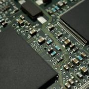
At their core, semiconductors are materials—typically silicon—with electrical conductivity between that of a conductor (like copper) and an insulator (like glass). This unique property allows semiconductors to control the flow of electric current, making them the building blocks for electronic circuits.
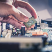
Semiconductors function by manipulating electrons through doping, a process where small amounts of impurities are added to the material to change its electrical properties. There are two main types of semiconductors:
- N-type semiconductors: Carry electric current via negatively charged electrons.
- P-type semiconductors: Rely on positively charged “holes” where electrons are absent.
When N-type and P-type semiconductors are combined, they form a PN junction—the basic structure behind transistors, diodes, and other essential electronic components. This junction allows semiconductors to switch, amplify, and regulate electrical signals, driving the functionality of complex Microsystems.
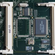
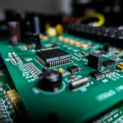
Why Semiconductors Matter in Microsystems
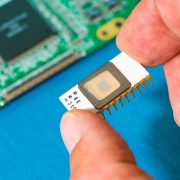
In Microsystems, semiconductors are crucial in miniaturizing and enhancing electronic devices. Their versatility allows for integrating multiple processing, memory, and communication functions into small, efficient chips. These compact semiconductor solutions power a wide range of applications, including:
- Medical devices: Enabling real-time patient monitoring and advanced diagnostics.
- Automotive technology: Supporting autonomous driving systems and vehicle sensors.
- Consumer electronics: Driving innovations in smartphones, wearables, and smart home devices.
Linear MicroSystems leverages cutting-edge semiconductor technology to create customized solutions for various industries, ensuring optimal performance, reliability, and energy efficiency.
Unlocking the Potential of Semiconductors with Microsystems
As demand for smaller, faster, and more efficient devices grows, semiconductors remain at the heart of technological progress. By harnessing the power of Microsystems, Linear MicroSystems designs next-generation semiconductor solutions tailored to our clients’ evolving needs.
Whether you’re developing innovative medical technology, advancing automotive systems, or creating more intelligent consumer electronics, our expertise in semiconductor design ensures your products stay ahead of the curve.
Interested in learning more about how semiconductors can revolutionize your technology? Contact Linear MicroSystems today to explore the possibilities.